


Contact series for contact mode and pulse force mode
Contact series for contact mode and pulse force mode
| Technical Data: | ||
| Value | Range | |
| Resonant Freq. | 13 kHz | +/-4 kHz |
| Force Constant | 0.2 N/m | 0.07 - 0.4 N/m |
| Length | 450 µm | +/-10 µm |
| Mean Width | 50 µm | +/-5 µm |
| Thickness | 2 µm | +/-1 µm |
| Tip Height | 17 µm | +/-2 µm |
| Tip Set Back | 15 µm | +/-5 µm |
| Tip Radius | <10 nm (Contact; ContAL; ContGD; ContGb) <25nm (ElectriCont) <15nm (ContDLC) Also see individual probes. |
|
| Half Cone Angle | 20°-25° along cantilever axis 25°-30° from side 10°-at the apex |
|


| Contact Tip radius <10nm | |
| Application: | Contact Mode, Pulsed Force Mode (PFM) |
| General: | Rotated Monolithic silicon probe Symetric Tip Shape Alignment Grooves (except for 1, see below) (Chipsize 3.4 x 1.6 x 0.3mm) |
| Coating: | None |

| ContAL Tip radius <10nm | |
| Application: | Contact Mode, Pulsed Force Mode (PFM) |
| General: |
Rotated Monolithic silicon probe |
| Coating: | 30nm Al for enhanced reflectivity |

| ContGD Tip radius <10nm | |
| Application: | Contact Mode, Pulsed Force Mode (PFM) |
| General: | Rotated Monolithic silicon probe Symetric Tip Shape Alignment Grooves (Chipsize 3.4 x 1.6 x 0.3mm) |
| Coating: | 70nm Au on back of cantilever |

| ContGB Tip radius <25nm | |
| Application: | Contact Mode, Pulsed Force Mode (PFM) |
| General: | Rotated Monolithic silicon probe Symetric Tip Shape Alignment Grooves (Chipsize 3.4 x 1.6 x 0.3mm) |
| Coating: | 70nm Au on both sides of cantilever |

| ElectriCont-G Tip radius <25nm | |
| Application: | Contact Mode, Pulsed Force Mode (PFM) and Electric Modes like: • Scanning Capacitance Microscopy (SCM) • Electrostatic Force Microscopy (EFM) • Kelvin Probe Force Microscopy (KFM) • Scanning Probe Lithography |
| General: | Rotated Monolithic silicon probe Symetric Tip Shape Alignment Grooves (Chip size 3.4 x 1.6 x 0.3mm) |
| Coating: | Electrically conductive Cr/Pt on both sides of cantilever. 5nm Cr covered with 25nm Pt. |
Contact Resistance: 300 ohms on Pt thin film surface

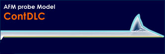
| ContDLC Tip radius <15nm | |
| Application: | Contact Mode |
| General: | Rotated Monolithic silicon probe Symmetric Tip Shape Alignment grooves (Chip size 3.4 x 1.6 x 0.3mm) |
| Coating: | Diamond-Like-Coating on tip side of cantilever, 15nm thick Aluminum Reflex coating on detector side of cantilever, 30nm thick This probe uses an "on scan angle" symmetric tip to provide a more symmetric representation of features over 200nm. |
Documentation
Documentation


0
Total items
0,00 lei
Taxes, discounts and shipping calculated at checkout.
Product subtotal